Can We See an Atom?
In this article, I will discuss how these images of atoms are made, what exactly we are looking at, and what it really means to see an atom. Over the decades there have been many attempts, claims, and misconceptions surrounding what atoms really look like and how we can photograph them. Let’s set that all straight below!
Table of Contents
Key Points
- We cannot see atoms with our eyes, or any device that enhances our eyes.
- Transmission Electron Microscopy (TEM) and Atomic Force Microscopy (AFM) are two methods used to image atoms.
- In TEM, electrons are sent through a sample and detected on the other side.
- AFM uses a platform with a very small tip and scans across a surface.
- Scanning Tunneling Microscopy (STM) uses a tip to shoot electrons out and measure the likelihood of electrons tunneling.
- Field Emission Microscopy, Field Ion Microscopy, and Atom Probe Tomography are other methods to image atoms.
- Atom Probe Tomography is a destructive technique that can image the 3D positions of atoms.
- Recent advances have allowed for a combination of TEM and computed tomography to image a 3D map of 27,000 atoms in a nanoparticle.
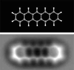
If you look on the internet for pictures of atoms, you will see images like this:
Or like this:
Or like this:
How do we see an atom?
The answer to the titular question really depends on what we mean by “see.” We see something when light emitted or reflected from an object reaches our eyes and the signal is sent to our brain.
The naked human eye has a resolution of about 100 microns. Atoms are separated by roughly a tenth of a nanometer, and we can barely see a mote of dust that is a million atoms wide. So in this sense, no we can not see an atom. But what if we use a magnifying glass? What if we use a microscope or a telescope? An electron microscope? Where do we draw the line of what it means to see something?
For the purposes of this article, I draw the line at visible frequency passive optics: lenses and mirrors. If a microscope is converting light to electrical signals or collecting data for longer than the human eye can, or the signal is being amplified digitally, or light is not being used at all, we are no longer seeing the object we are looking at, we are seeing what a computer screen is showing us.
So with our naked eyes, we cannot see atoms, and looking through any light microscope we also cannot, because even the best lenses and mirrors cannot beat the diffraction limit, which is roughly half a wavelength, about 200 nanometers, or 1000-2000 atoms. If materials existed that could refract X-rays like glass refracts visible light, we could maybe make an X-ray microscope, but those materials don’t exist.
Our eyes cannot see atoms, but what can?
Microscopy pronunciation
Microscopy isn’t pronounced like “microscope” with a y on the end; the first o is soft and the second o is a schwa, and the ‘cro’ (‘craw’) is stressed. It rhymes with colonoscopy: https://youtu.be/4c5ILWQmqRY?t=20
What is Transmission Electron Microscopy
The electron microscope images we usually see are from scanning electron microscopes (SEMs), which bounce a beam of electrons off a sample coated with metal. These do not have an atomic resolution. Transmission electron microscopes (TEMs) send a beam of electrons through a sample, and the electrons are detected on the other side. If SEMs are like a medical ultrasound, TEMs are like an x-ray.
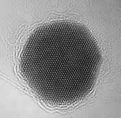
A simple way to interpret a TEM image is that where there is something brighter in the image, there is less stuff blocking the electrons. So if the resolution is high enough, and you see an image like:
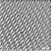
rather than seeing atoms in a plane, you are likely seeing the projected shadow of a column of atoms, rather than the shadow of an individual atom.

The bright spots on the image are regions where there are fewer atoms blocking the electrons. This is not quite how TEM imaging works, the electrons must be re-focused after going through the sample.
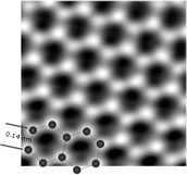
The technology has improved over the years, and now it is possible to perform TEM on single-layer graphene and see the atomic structure from a sheet of carbon, which I think is pretty impressive.
What is Atomic Force Microscopy
An atomic force microscope (AFM) is not an electron microscope, it is an example of a scanning probe microscope. Basically, it is a little platform (often big enough to see, like a few millimeters), with a very very small tip on the end. The platform and tip are dragged across a surface and a laser beam is reflected off the surface of the platform, and deflections in the platform deflect the beam, which can be recorded.
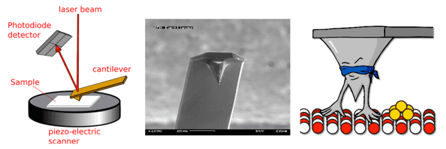
Left. Schematic of AFM operation. Middle: SEM image of an AFM cantilever and tip (source). Right: I’m not sure why this image exists but I wanted to include it (source).
There are two main ways that these operate. One is by having the platform vibrate up and down at the resonance frequency of the platform, called tapping mode. When something interacts with the tip, the frequency of the platform changes, and this is recorded. The other just keeps the tip at a constant height and measures the deflection of the platform as the tip is lifted by objects on the surface.

Everything is better as a GIF. Source.
The resolution of an AFM is basically determined by how sharp the tip is, and with a tip that truncates with a single atom, one can have an atomic resolution. So the way these images are made is by scanning an extremely sharp tip across a surface and measuring at each point either the force exerted on the tip or the height of the surface. The measurements can be fine enough to detect surface deflections caused by single atoms.
The tip generally scans in a straight line, then moves over slightly and scans again. On an atomically flat surface, each line looks like a zig-zag pattern, and by putting these together you get a 2D image (which you can 3D render if you want).
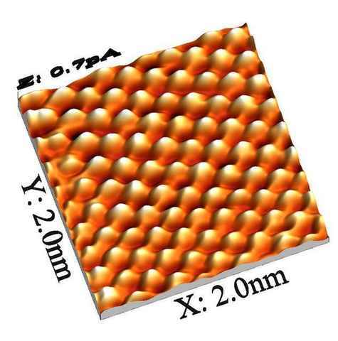
2 nm square image of the heights of atoms across a plane. Source.
This is the method that was used to image the organic molecule shown at the beginning of this article. It requires not only a very sharp tip but also hours and hours of extremely slow scanning. Very impressive.
What is Scanning Tunneling Microscopy
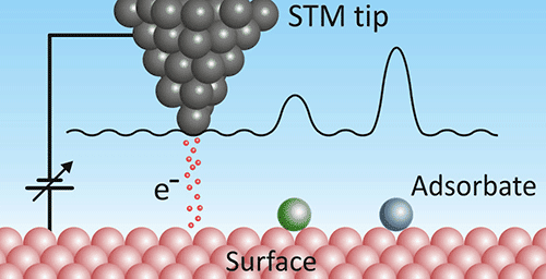
Another example of a scanning probe microscope, the scanning tunneling microscope (STM) looks similar to an AFM except instead of measuring the deflection of the tip, it shoots electrons out of the tip. The electrons are bound to the atoms in the tip, but a voltage is applied between the tip and the surface, making the electrons likelier to quantum tunnel from the tip to the surface. Instead of measuring height, the STM measures how likely at each point the electron is to tunnel (technically, the local density of states).
STM images are the most likely to be excessively 3D rendered by their creators, making it look like someone is holding a camera right next to an atom and taking a picture with a flash. I have a feeling this is because IBM invented the technique in the 1980s. One cool thing about STM is that the tunneling probability depends on the electron density of the surface, so you can actually visualize the wavefunction of the unbound surface electrons, in the images.
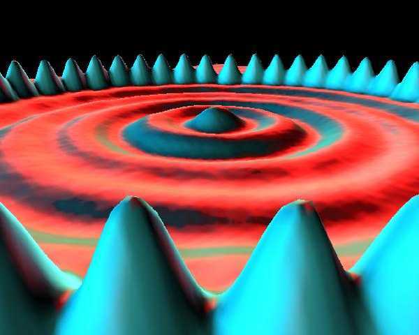
A boy and his atom: the world’s smallest movie
Field Emission Microscopy, Field Ion Microscopy, and Atom Probe Tomography
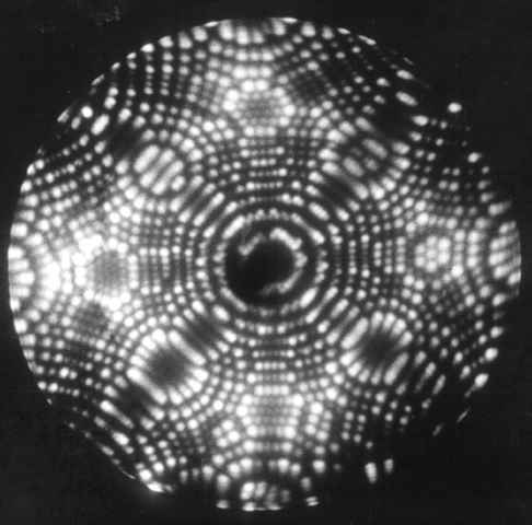
The surface of a platinum tip. The different rosettes of atoms are different crystal planes. Source.
One of the oldest techniques that could image with atomic resolution, field emission microscopy involves applying a massive voltage (thousands of volts) between a tungsten tip and a screen. The electrons start flying out of the tip, follow the non-uniform electric field, and hit the screen, where their position is noted and back-tracked to figure out where on the tip it came from. This can be used to ascertain the position of each atom in the tip.

A voltage is applied between the tip and the screen. Electrons fly off the tip, follow the electric field, and are back-tracked to determine the atomic organization of the tip.
There are other variants, including field ion microscopy, where atoms are adsorbed onto the tip and then flung off (rather than electrons), and atom probe tomography, which is a destructive technique that involves applying sufficient voltage to a sample that the individual atoms start flying off.
Atomic imaging: Now in 3D!
These techniques generally rely on locating the positions of atoms in a plane and then rendering them so that people can see where the atoms are. There are a few methods, however, that can image the 3D positions of atoms.
The aforementioned Atom Probe Tomography is an example: as each atom flies off the sample, its original position can be ascertained, and a 3D image of each atom’s location can be built up. It can also distinguish different elements. However, it is generally limited to things that are small and shaped like a narrow cone.

A Gallium/Indium cone. Source
I recently saw a video produced by Nature talking about a paper that effectively combined TEM with computed tomography (CT) imaging. They took a 2D TEM image of a nanoparticle at different angles and combined all the data to obtain a 3D map of the 27,000 atoms in the particle. I thought it was pretty cool.
Conclusion
We can’t see atoms with our eyes, or with anything, that enhances our eyes, but we can figure out the positions of atoms and render those in a way that we can see. The future is bright with new ideas and technology. In the decades coming, we may actually get images and pictures of atoms that laymen can wrap their heads around.
Update: Scientists now have a new image of the more detailed view of an atom here.
Related: Do we know what an electron looks like?
Ph.D. McGill University, 2015
My research is at the interface of biological physics and soft condensed matter. I am interested in using tools provided from biology to answer questions about the physics of soft materials. In the past I have investigated how DNA partitions itself into small spaces and how knots in DNA molecules move and untie. Moving forward, I will be investigating the physics of non-covalent chemical bonds using “DNA chainmail” and exploring non-equilibrium thermodynamics and fluid mechanics using protein gels.


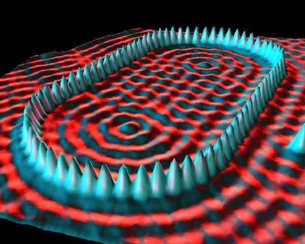




''the tunneling probability depends on the electron density of the surface, so you can actually visualize the wavefunction of the unbound surface electrons, in the images.'' The second half is not quite true, as the wave function of the electrons is a multiparticle wave function and we see something in 3 dimensions. What is visualized is the charge density of the electron field.
Kudos on your Insights article. Your explanations and graphics helped make it clear.
"Can We See an Atom?"Heck, I've never seen my face. I'm sure I got one.Have we ever seen the sun, much less other stars? We see their light, yet where are they when we finally perceive them? You can do the math; it's hurting my head to figure it. I am sure these heavenly bodies aren't where they were when we finally perceive their light.Have we seen the Higgs boson? <detour> Higgs boson walks into church. Priest says, we don't allow Higgs boson in here. Higgs boson says, yeah, but without me how can you have mass? </detour>Stick a fork in me. :)
How did Ernst Mach say: "Ah Atome! Ham's scho ans g'sehn?" (Ah atoms! Did you already see one?)
it depends whether they're dark field or bright field image.
Thanks!
Great job, Klotza!
Very interesting. But I'm confused with the image just below the text that reads: "The technology has improved over the years, and now it is possible perform TEM on single-layer graphene and see the atomic structure from a sheet of carbon, which I think is pretty impressive." This illustration pretty clearly shows carbon atoms as *light* spots, not dark spots. But the caption to the immediately previous image reads: "The bright spots on the image are regions where there are fewer atoms blocking the electrons."In a TEM image, are the atoms bright, or are they dark?
Glad you liked it!
Thank You for this really nice article !!
Wonderful article on the subject by Prof. Philip Moriarty(of SixtySymbols fame) from a couple of years ago.Recommended reading to all:http://www.nottingham.ac.uk/~ppzstm/pdfs/papers/2014/moriarty_visualizing.pdf
I've seen many of these "atom" photos online. Nice to get some explanations!